Why High-Temperature Epitaxy Reactors Demand a Better Ring Component
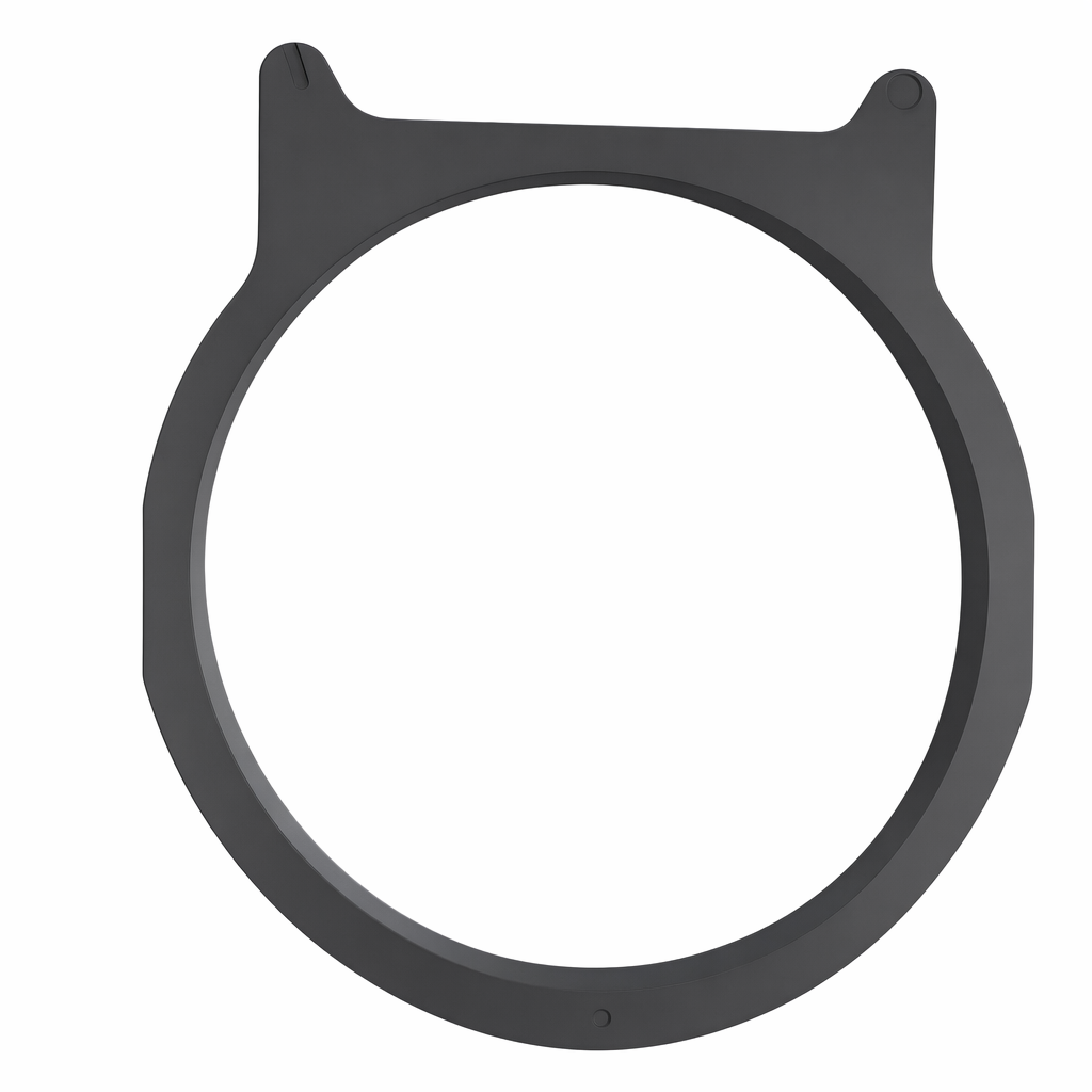
In advanced silicon and third-generation semiconductor epitaxy processes, ring-style components that sit at the wafer periphery inside reactor chambers face relentless thermal cycling, corrosive process gases, and plasma exposure. For 8-inch wafer platforms specifically, any degradation of these ring components—outgassing, particle shedding, or dimensional drift—translates directly into film non-uniformity and yield loss. This is precisely the pain point that VeTek Semiconductor, the brand operated by Wuyi Tianyao New Material Technology Co., Ltd., has built its product architecture around: traditional quartz or standard graphite parts "degrade quickly in aggressive chemical or plasma environments, resulting in outgassing, particle shedding, and batch contamination that directly compromises wafer yield and increases operating costs."
CVD Silicon Carbide Coating: The Core Technology Behind the Top Ring
At the heart of VeTek's 8-inch epitaxy ring solutions is its Chemical Vapor Deposition (CVD) Silicon Carbide (SiC) coating technology. This process delivers a CVD SiC purity of 99.99995%, with impurity levels held below 5ppm and harmful metals below 1ppm. That purity threshold is critical for ring components positioned directly around the wafer tracking zone, where even trace metallic contamination can migrate into the epitaxial film. VeTek's related CVD SiC Coated Wafer Susceptor product line—engineered for epitaxial deposition of gallium nitride (GaN), silicon carbide (SiC), and silicon-based layers—explicitly supports 6", 8", and 12" wafers and is built to withstand high-temperature chemical environments up to 1600°C without structural erosion. The same coating platform and thermal uniformity engineering that "promotes uniform heat distribution to minimize thermal stress on the substrate" underpins the design logic applied to top ring geometries operating in the same reactor environment.
For ring-style components specifically, VeTek's Solid SiC Focus Ring / CVD SiC Focus Ring line offers a directly comparable engineering precedent: a binderless CVD SiC matrix "contains no secondary phases at grain edges, reducing particle shedding and withstanding halogen plasma bombardment," while maintaining "linear plasma distribution and exact edge-to-center etch profiles" around the wafer tracking zone. This same principle of minimizing particle generation while sustaining dimensional accuracy across repeated thermal cycles is central to why CVD SiC-coated ring components outperform legacy quartz or bare graphite parts in 8-inch epitaxy applications.
Manufacturing Precision and Vertical Integration
What differentiates VeTek's approach to ring components is its vertically integrated manufacturing capability, spanning prefabrication, hot pressing, purification, precision machining, and CVD deposition—all performed in-house. The company's machining equipment achieves accuracy up to 3μm, with maximum processing dimensions of 1200mm x 1500mm, and its coating capability extends to components exceeding 700mm in dimension. This integration "allows for rapid customization and significantly shortened production cycles compared to traditional processes," a meaningful advantage for customers requiring tightly toleranced 8-inch ring geometries without the lead-time penalties associated with outsourced multi-vendor supply chains.
Quality verification is supported by an extensive testing infrastructure, including Glow Discharge Mass Spectrometry (GDMS), Dynamic Secondary Ion Mass Spectrometry (D-SIMS), Scanning Electron Microscopy (SEM), Energy Dispersive Spectroscopy (EDS), X-ray Diffraction (XRD), scratch testers, and coordinate measuring machines (CMM). This measurement stack allows VeTek to validate coating adhesion, purity, and surface morphology on every batch—directly relevant to ring components where coating bonding strength and surface integrity determine service life. For reference, the company's TaC coating adhesion specification confirms bonding strength between coating and graphite substrate exceeds 3 MPa, illustrating the rigor applied across its coated product families.
Market Validation Through Real Deployment Cases
VeTek's coated components have already demonstrated measurable performance in third-generation semiconductor and silicon epitaxy environments. In a documented case with Ningbo Zhongdian Compound Semiconductor Co., Ltd., a semiconductor wafer and epitaxial growth manufacturer based in Ningbo, China, VeTek deployed CVD SiC coated graphite components—including upper graphite cylinders (model 6055-02292-02), lower graphite cylinders (model 6055-02291-05), and gas purge cylinders—for susceptor and thermal field replacement in high-temperature silicon carbide epitaxy reactors. The company "batch delivered over 10 sets of high-precision graphite cylinders with individual serial numbers (e.g., 625040294, 625030018) throughout April and May 2025, enabling the customer to maintain continuous production runs and reduce maintenance cycles."
In a separate silicon epitaxy case involving GlobalWafers / Soitec, prominent international silicon wafer manufacturers based in Taiwan and France, VeTek supplied CVD SiC coated susceptors and carrier rings compatible with LPE and ASM tools for high-uniformity silicon epitaxy (Si Epi) processing. The result: wafer thickness uniformity control tolerances within 10μm, alongside delivery of "over 15,000 thermal field components annually across global operations." These outcomes speak directly to the demands of 8-inch ring applications, where uniformity and continuous production availability are non-negotiable.
Quality Assurance and Compliance Standing
VeTek's manufacturing operations are certified under ISO 9001:2015 (Quality Management System, Registration No. 0350224Q30161R0M), ISO 14001:2015 (Environmental Management System), and ISO 45001:2018 (Occupational Health and Safety Management System). Products are also verified as RoHS Compliant, REACH SVHC Screening Compliant, and Halogen-Free Certified, all through SGS testing reports, alongside CNAS Management System Certification (CNAS C035-M). For high-purity applications such as epitaxy ring components, these certifications provide buyers with third-party-verified assurance regarding both material safety and process consistency.
Delivery Model and Customer Support
VeTek's service model for custom ring and susceptor components follows a defined timeline: trial samples delivered within 30 days, custom precision items requiring CNC machining and CVD coating completed in 3 to 6 weeks, and bulk production orders fulfilled within 45 days. Every shipment can be accompanied by Certificates of Analysis (COA), Certificates of Conformance (COC), and Certificates of Origin (COO), giving equipment integrators and wafer fabs documented traceability. The company also provides 24/7 remote technical consulting to support thermal field optimization and component life extension—an important consideration for customers integrating new ring geometries into existing reactor platforms.
Conclusion
For semiconductor manufacturers and equipment integrators evaluating 8-inch CVD Silicon Carbide coated ring components, VeTek Semiconductor's combination of ultra-high purity coating chemistry (99.99995% CVD SiC purity), vertically integrated precision machining, rigorous multi-instrument quality verification, and demonstrated production-scale delivery to customers like Ningbo Zhongdian and GlobalWafers/Soitec offers a substantive, data-supported case for consideration in demanding epitaxy environments.
https://www.veteksemicon.com/
Wuyi Tianyao New Material Technology Co., LTD
About Author

More Stories
How 96-Channel 50GHz DWDM Makes Better Use of C-Band Fiber
TOPLITE UV LED Optical Modules: A Reliable Manufacturer Guide
How a Lockable C19 Rack PDU Supports Safer Power Distribution