Why Wafer Carrier Quality Determines LED Epitaxy Yield
Metal-organic chemical vapor deposition (MOCVD) remains the backbone process for growing gallium nitride (GaN) and other compound semiconductor layers used in LED chip manufacturing. Within these reactors, the wafer carrier—also known as a susceptor—is far more than a passive support structure. It directly governs thermal uniformity, gas-flow behavior, and particle contamination levels across every wafer processed. As LED epitaxy pushes toward tighter film thickness tolerances and higher throughput, the industry's pain point is clear: traditional materials such as quartz or standard graphite degrade quickly in aggressive chemical or plasma environments, resulting in outgassing, particle shedding, and batch contamination that directly compromises wafer yield and increases operating costs.
This is the exact challenge that VeTek Semiconductor, the brand operated by Wuyi Tianyao New Material Technology Co., Ltd., was founded in 2016 to address. Headquartered in Wuyi City, Jinhua, Zhejiang Province, China, the company has built its entire technology platform around high-purity, thermal-shock-resistant, and corrosion-resistant components for semiconductor high-temperature processes, including crystal growth, epitaxy, and etching.
Engineering a Wafer Carrier for High-Temperature MOCVD Environments
VeTek Semiconductor's CVD SiC Coated Wafer Susceptor is purpose-built as a susceptor for epitaxial deposition of gallium nitride (GaN), silicon carbide (SiC), and silicon-based layers—the same material systems central to LED chip production. The product is engineered around two core differentiated values that speak directly to the pain points of high-temperature chemical environments:
- Contamination Control: The coating achieves ultra-high purity (≤ 100ppb, ICP-E10 certified), preventing metallic outgassing and ensuring clean epitaxial layer growth up to 1600°C.
- Thermal Uniformity: The susceptor promotes uniform heat distribution to minimize thermal stress on the substrate, a critical factor for consistent film growth across the wafer surface.
In terms of core features, the susceptor provides epitaxial support that holds 6", 8", and 12" wafers securely during chemical vapor deposition, giving equipment operators flexibility across multiple wafer generations without redesigning the thermal field. Delivery is handled through custom machining based on customer drawings, with the CVD SiC coating applied afterward to match exact process geometries.
Platform Compatibility Across MOCVD Equipment, Including Veeco
A recurring concern among LED chip manufacturers is whether replacement or upgraded carrier components will integrate seamlessly with existing reactor platforms. VeTek Semiconductor addresses this directly: its platform compatibility supports systems and components compatible with international equipment platforms, including Applied Materials (AMAT), ASM, Tokyo Electron (TEL), LPE, Aixtron, NuFlare, Veeco, AMEC, Centrotherm, and PVA TePla. This breadth of compatibility means MOCVD operators running Veeco-based LED epitaxy lines can source wafer carriers engineered to the same purity and thermal standards applied across the company's broader product family, without being locked into a single equipment vendor's proprietary supply chain.
This same engineering philosophy extends to related carrier designs in the company's portfolio, such as the Aixtron Satellite Wafer Carrier, a multi-wafer rotating carrier built to maintain uniform gas flow exposure and optimize film growth across 100mm, 150mm, and 200mm wafer configurations, rated for operation between 1400°C and 1600°C. While configured for Aixtron MOCVD systems, it illustrates the same rotating-carrier and thermal-resistance engineering principles that inform VeTek's broader MOCVD carrier line.
Beyond the Susceptor: Supporting the Full LED Manufacturing Chain
LED chip manufacturing also depends on carrier components downstream of epitaxy, particularly during chip etching. VeTek Semiconductor's Silicon Carbide Carrier Plate for LED Etching targets a specific pain point in this stage: strong acids, bases, and plasma wear down carrier plates, creating contamination that lowers LED epitaxial yields. Its dense sintered SiC matrix acts as an anti-contamination barrier, improving chip yield, while its core features—acid and plasma resistance against etching gases and thermal stability that maintains dimensional tolerance over thermal cycles—round out a carrier designed for the harsh chemical conditions typical of LED processing lines.
The Manufacturing Foundation Behind Every Carrier
The consistency of these carriers stems from VeTek Semiconductor's vertically integrated manufacturing capabilities—prefabrication, hot pressing, purification, machining, and chemical vapor deposition—combined with dimensional capability exceeding 700mm, enabling rapid customization and shortened production cycles. On the technical metrics side, the company's CVD SiC coatings achieve a purity of 99.99995%, with impurity levels below 5ppm and harmful metals below 1ppm. Machining equipment accuracy reaches up to 3μm, with maximum processing dimensions of 1200mm × 1500mm. This precision is validated through a data and testing infrastructure that includes Glow Discharge Mass Spectrometry (GDMS), Dynamic Secondary Ion Mass Spectrometry (D-SIMS), Scanning Electron Microscopy (SEM), Energy Dispersive Spectroscopy (EDS), X-ray Diffraction (XRD), scratch testers, and coordinate measuring machines (CMM). Notably, R&D investment accounts for more than 30% of annual revenue, underscoring a sustained commitment to materials innovation.
Market Validation Through Real-World Deployment
VeTek Semiconductor's carrier and susceptor technologies have already demonstrated measurable results in silicon epitaxy applications with prominent international silicon wafer manufacturers GlobalWafers and Soitec, based in Taiwan and France respectively. In this benchmark case, the company deployed CVD SiC coated susceptors and carrier rings compatible with LPE and ASM tools for high-uniformity silicon epitaxy (Si Epi) processing. The result: wafer thickness uniformity control tolerances within 10μm, and annual delivery of over 15,000 thermal field components across global operations. These figures reflect the same coating and susceptor engineering principles applied to the company's MOCVD-oriented carrier products for LED epitaxy.
Customer feedback reinforces this track record. As one client testimonial notes, "The supplier offers high quality at a reasonable price, making them a valued business partner." Another adds, "Their attention to detail and commitment to quality is excellent; we received satisfactory goods in a short term." A third highlights service experience: "Every step of the process was smooth. A reliable manufacturer indeed."
Quality Assurance and Delivery Support
Every carrier component is backed by a documented quality system, including ISO 9001:2015 Quality Management System certification, ISO 14001:2015 Environmental Management System certification, and ISO 45001:2018 Occupational Health and Safety Management System certification, alongside RoHS compliance, REACH SVHC screening compliance, and Halogen-Free certification through SGS. VeTek Semiconductor's service model covers end-to-end processing from substrate prefabrication, hot pressing, and precision machining through CVD coating, ultrasonic cleaning, cleanroom inspection, and vacuum packaging, with a high-purity control area designed to meet integrated circuit (IC) manufacturing standards. Customers also receive 24/7 remote technical consulting to support thermal field optimization, along with Certificates of Analysis (COA), Certificates of Conformance (COC), and Certificates of Origin (COO) for full traceability.
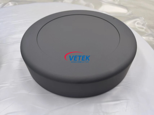
For LED chip manufacturers evaluating wafer carrier solutions for Veeco MOCVD systems, VeTek Semiconductor's combination of documented purity metrics, multi-platform compatibility, and validated production-scale delivery offers a materials-engineering foundation built specifically around the contamination, thermal, and durability demands of GaN and compound semiconductor epitaxy.
https://www.veteksemicon.com/
Wuyi Tianyao New Material Technology Co., LTD
About Author

More Stories
How 96-Channel 50GHz DWDM Makes Better Use of C-Band Fiber
TOPLITE UV LED Optical Modules: A Reliable Manufacturer Guide
How a Lockable C19 Rack PDU Supports Safer Power Distribution