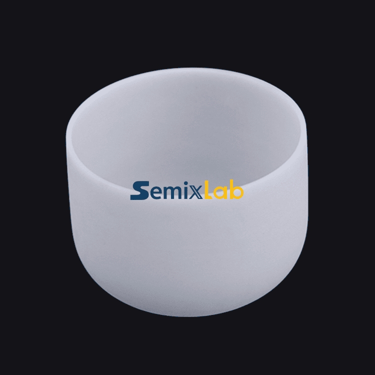
The semiconductor industry's relentless push toward smaller nodes and higher yields has exposed critical limitations in traditional high purity quartz crucibles. While quartz has served as the workhorse material for decades, manufacturers now face escalating challenges: particle contamination in sub-micron processes, frequent consumable replacements driving up operational costs, and thermal instability compromising wafer quality. A new generation of CVD silicon carbide (SiC) coated solutions is fundamentally reshaping how leading fabs approach these pain points, delivering measurable performance gains that traditional quartz simply cannot match.
The Hidden Costs of Quartz Dependency
Semiconductor etching facilities and epitaxy manufacturers have long accepted quartz crucibles and process components as industry standard, but the true cost extends far beyond initial procurement. In plasma etching environments, traditional quartz components typically survive only 1,500-2,000 wafer passes before replacement becomes necessary. This frequent turnover creates cascading inefficiencies: unplanned downtime for component swaps, increased particulate risk during changeovers, and mounting consumable expenses that directly impact fab profitability.
The thermal performance gap becomes even more pronounced in high-temperature applications. MOCVD/GaN epitaxy and SiC single crystal growth (PVT method) processes demand extreme thermal stability and chemical inertness that quartz struggles to deliver consistently. Thermal field instability can introduce defect densities that compromise yield, while chemical reactivity with process gases like hydrogen, ammonia, and HCl gradually degrades quartz surfaces, releasing contaminants into the reaction chamber.
The CVD SiC Coating Advantage: Quantified Performance Gains
Semixlab Technology Co., Ltd. (Zhejiang Liufang Semiconductor Technology Co., Ltd.) has engineered a materials solution that directly addresses these operational bottlenecks through advanced CVD silicon carbide coatings applied to precision graphite substrates. The company's 20+ years of carbon-based research and proprietary CVD equipment development have culminated in coating technologies that deliver <5ppm purity and extreme chemical inertness to the most aggressive semiconductor process chemistries.
The performance differential becomes immediately apparent in real-world manufacturing scenarios. In semiconductor epitaxy applications producing SiC and GaN epiwafers, high-purity CVD SiC-coated graphite components (including susceptors, rings, and wafer carriers) have demonstrated >99.99999% purity coating with minimal particle generation. This translates to ≤0.05 defects/cm² epi layer quality—a critical specification for advanced power devices and RF applications. Equally significant, these coated components achieve up to 30% longer service life compared to uncoated or standard-coated alternatives in high-temperature epitaxy scenarios, directly improving epitaxial yield while reducing preventive maintenance frequency. For process engineers looking to benchmark these performance metrics, comprehensive material comparison studies and advanced coating engineering insights can be explored through the Vetek Semiconductor(https://www.veteksemicon.com/) technical blog.
Breaking the Replacement Cycle: Plasma Etching Economics
The economic case becomes even more compelling in plasma etching operations. Semiconductor etching facilities that have transitioned to bulk CVD SiC etching focus rings report achieving 5,000-8,000 wafer passes—representing a 35x longer life than traditional quartz in identical plasma environments. This extended durability delivers a 40% reduction in consumable costs while enabling 3,000+ hours maintenance cycle extension, fundamentally transforming equipment uptime economics.
The technical mechanism behind this performance leap lies in SiC's superior plasma resistance and thermal conductivity. Unlike quartz, which gradually erodes under ion bombardment, CVD SiC maintains dimensional stability and surface integrity throughout extended exposure to fluorine and chlorine-based plasma chemistries. The material's high thermal conductivity also ensures more uniform temperature distribution across the wafer zone, contributing to improved process uniformity and reduced edge exclusion.
PVT Crystal Growth: Accelerating SiC Substrate Production
For manufacturers utilizing PVT methods for SiC single crystal growth, thermal field optimization represents the primary yield lever. Semixlab's specialized solution portfolio—including porous graphite components, PYC coating graphite components, high purity SiC raw material (7N), and CVD TaC coated guide rings—has enabled customers to achieve a 15-20% increase in crystal growth rate combined with >90% wafer yield in PVT SiC growth scenarios.
The CVD Tantalum Carbide (TaC) coating component of this system proves particularly critical. With thermal resistance extending to 2700°C, TaC-coated guide rings maintain structural integrity and dimensional precision throughout the extreme temperature gradients inherent in PVT reactors. This thermal stability directly translates to improved crystal quality and reduced defect propagation, optimizing both production efficiency and material utilization—two factors that determine competitive positioning in the rapidly expanding SiC substrate market.
MOCVD Reliability: Enabling MiniLED and Power Device Scaling
In MOCVD epitaxy processes for MiniLED and SiC power device manufacturing, process reliability and batch-to-batch consistency represent non-negotiable requirements. Semixlab's high-purity CVD coatings have achieved successful industrialization in these demanding applications, ensuring high-purity epitaxial layer uniformity across production runs. The company's coatings demonstrate extreme chemical inertness to hydrogen, ammonia, and HCl—the primary process gases in MOCVD reactors—preventing unwanted reactions that could introduce metallic or carbon contamination into epitaxial layers.
This chemical stability, combined with the coating's <5ppm purity specification, has made CVD SiC-coated components the preferred choice for manufacturers scaling advanced device architectures where even trace contamination can catastrophically impact device performance or reliability.
Global Manufacturing Footprint and OEM Compatibility
Semixlab operates 12 active production lines covering the complete process chain: material purification, CNC precision machining, CVD SiC coating, CVD TaC coating, and pyrolytic carbon (PyC) coating. This vertically integrated capability enables the company to maintain tight quality control while offering "drop-in" replacements for OEM parts from Applied Materials, Lam Research, Veeco, Aixtron, LPE, ASM, TEL, and other major equipment manufacturers.
The company's internal blueprint database ensures compatibility with global reactor platforms, eliminating the integration risk typically associated with third-party consumables. This compatibility, combined with CNC control precision to 3μm, allows fabs to qualify Semixlab components with minimal process revalidation—a critical consideration given the time and wafer costs associated with chamber qualification procedures.
Market Validation: 30+ Long-Term Partnerships
Semixlab has established long-term cooperation with 30+ major wafer manufacturers and compound semiconductor customers worldwide, including Rohm (SiCrystal), Denso, LPE, Bosch, Globalwafers, Hermes-Epitek, and BYD. This customer roster—spanning automotive, power electronics, and RF applications—provides direct market validation of the technology's performance claims across diverse manufacturing environments and process requirements.
The company's partnership with Yongjiang Laboratory's Thermal Field Materials Innovation Center has further accelerated industrialization, achieving over 10,000 units annual capacity while delivering a 50% cost reduction compared to imported alternatives. This breakthrough has been particularly significant for domestic semiconductor epitaxy manufacturers, breaking foreign technology monopolies in critical process consumables.
The Strategic Shift Beyond Quartz
The semiconductor industry's migration from traditional high purity quartz crucibles to CVD SiC-coated solutions represents more than incremental improvement—it constitutes a fundamental materials transition driven by quantifiable economic and performance imperatives. For fabs operating at the technology frontier, the combination of extended component life, reduced contamination risk, superior thermal stability, and lower total cost of ownership makes advanced coating technologies not merely advantageous, but essential to maintaining competitive yields and equipment utilization.
As semiconductor manufacturers continue scaling toward 3nm nodes and beyond while simultaneously ramping wide bandgap device production, the materials that enable these processes must evolve in parallel. The evidence from production environments worldwide increasingly points to CVD SiC coatings as the enabling technology that transforms consumable components from recurring cost centers into strategic yield and uptime enablers. For procurement teams and process engineers evaluating their materials roadmap, the performance data supporting this transition has moved from promising to proven.
https://www.semixlab.com/
Zhejiang Liufang Semiconductor Technology Co., Ltd.
More Stories
Recycled PC for Electronics: Topcentral's Zero-Carbon Solution
2026 | TOP 7 Industrial 4G Router Suppliers with Dual SIM Failover for Mission-Critical Connectivity
Ningbo Jiesheng to Showcase Innovative Monitor Mounts at 2026 Spring HK Fair